AluminaAl₂O₃
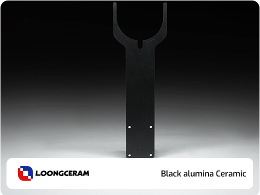
黑色氧化铝陶瓷
黑色氧化铝具有极低的反射率,同时保持了标准氧化铝的机械性能。目前,半导体和显示器制造设备中使用的氧化铝颜色主要为白色或象牙色,当用作光源周围或焦平面附近的组件时,由于反射光线而导致眩光,因此存在问题。黑色氧化铝能够抑制表面光反射,同时保持精细陶瓷所特有的强度和耐久性。(在240至2600纳米波长范围内,反射率为5.1%至15.3%)。黑色氧化铝可在300℃的温度下工作,因此具有足够的强度和耐久性,能够承受光源附近严苛的高温环境。
Jump to
核心特性
优异的遮光和防反射性能:保持光信号的纯度
传统的白色氧化铝陶瓷具有半透明性,光线可以轻易穿过。这种特性会对光敏器件(例如光学传感器和图像传感器)造成干扰。相比之下,黑色氧化铝陶瓷的表面光反射率更低,可以有效减少杂散光,防止光线反射到器件腔内的芯片表面,从而提高激光输出光的纯度和光电检测的信噪比。
这正是其在激光模块封装、相机模块和光敏传感器等领域的关键价值所在。
优异的散热性能:快速散热
黑色氧化铝由于在烧结过程中添加了导热系数更高的碳基或金属氧化物颗粒,因此具有更强的红外吸收和热辐射能力。这一特性不仅提高了材料的整体导热系数,而且能够在高功率封装中更快地散热,显著降低器件内部的热应力积累,维持器件温度稳定,从而延长使用寿命并提高系统可靠性。
高电磁屏蔽效率:芯片的“隐形保护层”
通过特殊的掺杂体系或微结构设计,黑色氧化铝能够在保持电绝缘性的同时吸收和反射电磁波,从而实现有效的电磁干扰(EMI)屏蔽。它不仅可以防止内部信号泄漏,还能抵御外部干扰波,确保设备运行的稳定性和可靠性。
注意:并非所有黑色氧化铝材料都具有显著的EMI屏蔽能力。功能性封装需要优化设计,例如添加导电相或碳掺杂
| 性能参数 | 单位 | 测试标准 | 数值 | |
| 密度 | [g/cm³] | JIS R 1634 | 4.9 | |
| 吸水率 | [%] | JIS C 2141 | 0 | |
| 维氏硬度 HV9.807N | [GPa] | JIS R 1610 | 6 | |
| 弯曲强度(三点弯曲) | [MPa] | JIS R 1601 | 130 | |
| 抗压强度 | [MPa] | JIS R 1608 | – | |
| 杨氏弹性模量 | [GPa] | JIS R 1602 | 160 | |
| 泊松比 | [-] | JIS R 1602 | – | |
| 断裂韧性(SEPB 法) | [MPa·m⁰·⁵] | JIS R 1607 | 1.1 | |
| 线膨胀系数 | 40 – 400 ℃ | [×10⁻⁶/K] | JIS R 1618 | 7.2 |
| 40 – 800 ℃ | [×10⁻⁶/K] | JIS R 1618 | 7.6 | |
| 热导率 | [W/(m·K)] | JIS R 1611 | 14 | |
| 比热容 | [J/(g·K)] | JIS R 1611 | 0.45 | |
| 抗热震温差 | [℃] | JIS R 1648 | – | |
| 介电强度 | [kV/mm] | JIS C 2141 | 11 | |
| 体积电阻率 | 20 ℃ | [Ω·cm] | JIS C 2141 | >10¹³ |
| 300 ℃ | [Ω·cm] | JIS C 2141 | 10¹⁰ | |
| 500 ℃ | [Ω·cm] | JIS C 2141 | 10⁷ | |
| 介电常数 | – | JIS C 2141 | 11 | |
| 介电损耗角 | [×10⁻⁴] | JIS C 2141 | 5 | |
| 损耗因数 | [×10⁻⁴] | JIS C 2141 | 55 | |
应用领域
激光二极管封装和光电探测器模块:黑色氧化铝陶瓷作为基板或间隔层,可以有效吸收内部杂散光,提高激光输出光束的纯度,同时保证封装的高绝缘性和机械稳定性,增强器件的长期可靠性。
黑色氧化铝陶瓷零件
相机模块黑色支撑片/遮光垫:用于微型相机和投影模块等光学元件中,用作遮光垫和结构支撑材料,有效减少光反射和交叉光干扰,防止图像出现眩光和重影,从而保证成像的清晰度和色彩准确性。
微型传感器封装外壳、芯片基板:在MEMS传感器、光学传感器或高精度微电子模块中,黑色氧化铝陶瓷可用作封装外壳或芯片基板。其材料特性不仅与芯片的热膨胀系数相匹配,具有可靠的气密性,而且还能承受热冲击和机械应力,阻挡外部光干扰,并确保传感器性能的稳定性。
黑色氧化铝陶瓷真空包装
真空封装和 MEMS 器件黑色基板:在真空封装或 MEMS 系统中,黑色氧化铝陶瓷基板不仅提供了坚固耐高温的结构支撑,还具有光学遮光和电磁干扰屏蔽的功能,为精密元件提供了全面的保护。
Alumina Machining
Alumina can be produced in various purities by adding additives to enhance its performance. The common purity range is from 90% to 99.9%, but Longci Ceramics typically use materials with a purity of 99.7%.
It can be processed by injection molding, compression molding, isostatic pressing, grouting molding and extrusion molding, etc. After sintering, processing can only be carried out using the diamond grinding method. The advanced green body and blank processing technology developed by Precision Ceramics Company enables the manufacture of more complex components using traditional processing methods. In addition, alumina can be easily bonded to metals or other ceramics through metallization and brazing techniques.
Alumina can be processed in green billets, billets or in a completely dense state. In the green or billet state, alumina can be processed into complex geometric shapes relatively easily. However, in order to fully densify the material, the sintering process will cause the alumina green body to shrink by approximately 20%. This shrinkage means that when processing alumina before sintering, very strict tolerances cannot be maintained. To achieve very strict tolerances, diamond tools must be used to process/grind fully sintered materials. During this manufacturing process, very precise diamond-coated tools/grinding wheels are needed to grind the material until the desired shape is formed. Due to the inherent toughness and hardness of the material, this can be a time-consuming and costly process.
CeramicMaterials
Forming method
Sutech has 5 molding techniques: dry pressing, high pressure injection olding, low pressure injection molding, Isostatic pressing molding, gel casting molding.In accord with customers specific structure, size, accuracy and quantity requirements, we choose suitable molding technique.
- Injection Molding+
- Extrusion Molding+
- Isostatic Pressing+
- Grouting Molding+
- Advantage+